


详情
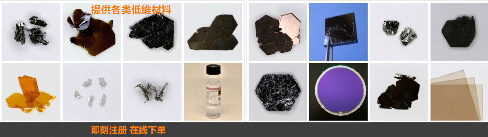
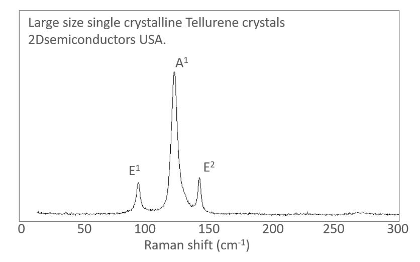
The first commercial vdW Tellurium (b-phase) crystals. Layered tellurium crystals have been synthesized in perfectly vdW order through flux zone growth technique. The crystal has 99.9999% (6N) rated purity and has been crystalized in perfect atomic order. Layered tellurium (Te) has a trigonal crystal lattice (see product images) in which individual helical chains of Te atoms are stacked together by van der Waals type bonds and spiral around axes parallel to the [0001] direction at the center and corners of the hexagonal elementary cell [1-2]. Tellurene exhibits a tunable bandgap varying from nearly direct 0.31 eV (bulk) to indirect 1.17 eV (2L) and direct at 1.3 eV (1L) [3]. It has been shown to exhibit metallic behavior under certain conditions and even host DCWs. It has four (two) complex, highly anisotropic and layer-dependent hole (electron) pockets in the first Brillouin zone with an extraordinarily high hole mobility reaching up to theoretical ∼1E5 cm2/Vs value [1-3].

Physical size ~1cm or larger;
Note: This product is same as tellurene material. While material itself is perfectly crystallized in trigonal form (weakly coupled Te chains are present), it is inherently harder to exfoliate in comparison to graphene or MoS2. For best results, we recommend using strongly adhesive tapes or liquid exfoliation technique.
Related references
[1] "Two-dimensional tellurium" Nature 552, 40-41 (2017)
[2] "Large-area solution-grown 2D tellurene for air-stable, high-performance field-effect transistors"; arXiv:1704.06202
[3] "Few-layer Tellurium: one-dimensional-like layered elementary semiconductor with striking physical properties"


7天即到
本地发货
满500元
免运费

支持信用卡在线支付
和银行转账

客服电话:400-701-7100
Email: taizhou@sunano.com.cn
 陈谷一
陈谷一