


详情
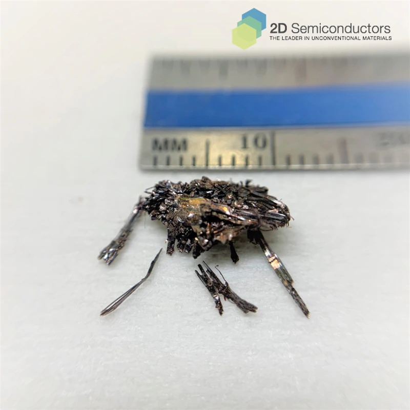
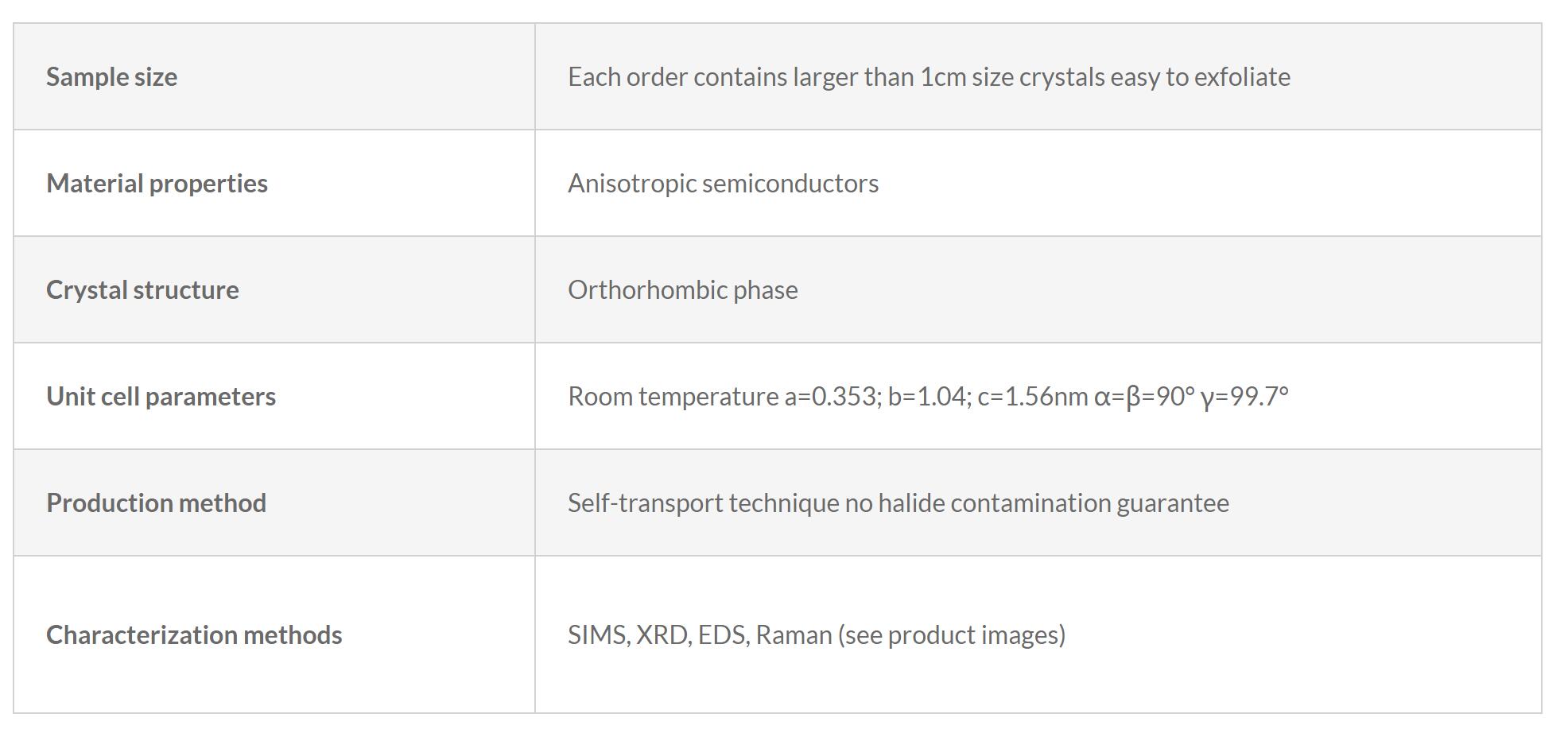
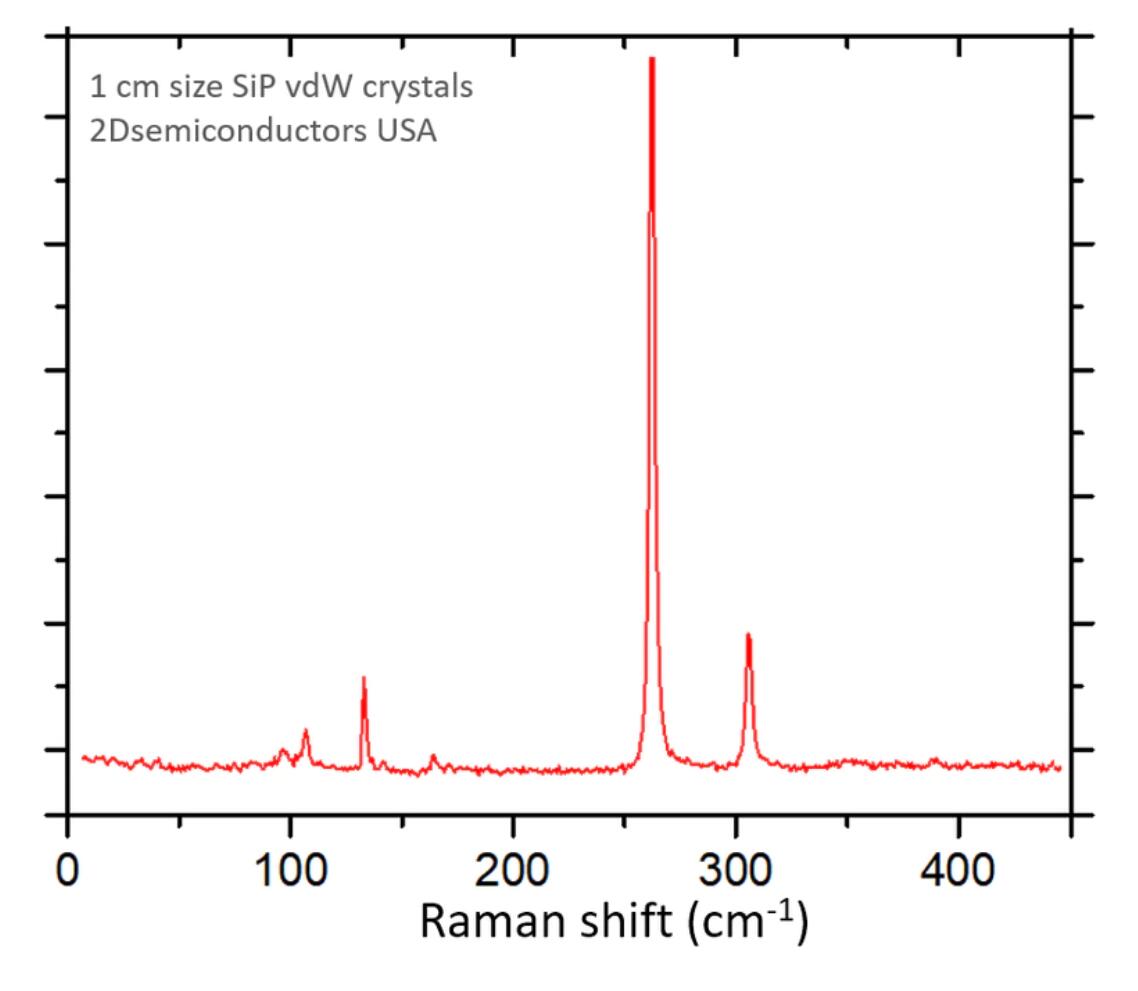
Silicon phosphide (SiP) is a layered semiconductor crystallizing in 2D anisotropic / orthorhombic crystal phase. It has been shown to undergo indirect (bulk) to direct (monolayer) gap transition from 1.69 (bulk) to 2.5 eV (monolayer). The atoms are arranged to form 1D-like features much similar to BLACK PHOSPHORUS, BLACK ARSENIC, GATE, and RES2. Owing to its highly anisotropic atomic arrangement, it has been shown to host anisotropic excitons, thermal conduction, optical absorption, as well as electronic mobility. Our SiP crystals are grown using two different techniques through chemical vapor transport (CVT) or flux zone growth (see description of these two methods below). These crystals are treated as gold standards in 2D materials field owing to perfected optical and electronic behavior. SiP crystals appear to be fibrous (microscale layered ribbons) that are ready for exfoliation as shown in the images.
Growth method matters Contamination of halides and point defects in layered crystals are well known cause for their reduced electronic mobility, reduced anisotropic response, poor e-h recombination, low-PL emission, and lower optical absorption. Self-transport growth technique is a halide free technique used for synthesizing truly semiconductor grade vdW crystals. This method distinguishes itself from chemical vapor transport (CVT) technique in the following regard: CVT is a quick (~2 weeks) growth method but exhibits poor crystalline quality and the defect concentration reaches to 1E11 to 1E12 cm-2 range. In contrast, self-transport method takes long (~1-2 months) growth time, but ensures slow crystallization for perfect atomic structuring, and impurity free crystal growth with defect concentration as low as 1E9 - 1E10 cm-2. During check out just state which type of growth process is preferred. Unless otherwise stated, 2Dsemiconductors ships Flux zone crystals as a default choice.


7天即到
本地发货
满500元
免运费

支持信用卡在线支付
和银行转账

客服电话:400-701-7100
Email: taizhou@sunano.com.cn
 陈谷一
陈谷一