


详情
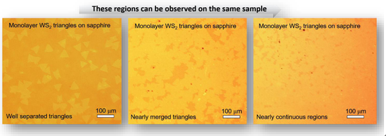
Isolated monolayer thickness WS2 are grown onto c-cut (0001) sapphire substrates. This particular product contains monolayer thickness WS2 triangular flakes randomly distributed across sapphire substrate. While some regions reach continuity with coalesced WS2 triangles, this sample contains well-separated triangles for advanced spectroscopy, microscopy, and electronic measurements. Synthesized monolayer WS2 triangles are highly luminescent and Raman spectroscopy studies also confirm the monolayer thickness.
Sample Properties.
Sample size |
1cm x 1cm square shaped |
Substrate type |
(0001) c-cut sapphire |
Coverage |
Isolated and partially merged monolayer triangl |
Electrical properties |
2.0 eV Direct Bandgap Semiconductor |
Crystal structure |
Hexagonal Phase |
Unit cell parameters |
a = b = 0.312 nm, c = 1.230 nm, α = β = 90, γ = 120° |
Production method |
Low pressure Chemical Vapor Deposition (LPCVD) |
Characterization methods |
Raman, photoluminescence, TEM, EDS |
Specifications
1) Identification. Well-separated WS2 domains across c-cut sapphire
2) Physical dimensions. One centimeter in size. Larger sizes up to 2-inch wafer-scale available upon requests.
3) Smoothness. Atomically smooth surface with roughness < 0.2 nm.
4) Uniformity. Highly uniform surface morphology. WS2 triangles are scattered across sample.
5) Purity. 99.9995% purity as determined by nano-SIMS measurements
6) Reliability. Repeatable Raman and photoluminescence response
7) Crystallinity. High crystalline quality, Raman response, and photoluminescence emission comparable to single crystalline monolayer flakes.
8) Substrate. c-cut Sapphire but our research and development team can transfer WS2 triangles onto variety of substrates including PET, quartz, and SiO2/Si without significant compromising of material quality.
9) Defect profile. WS2 monolayer triangles do not contain intentional dopants or defects. However, our technical staff can produce defected WS2 using α-bombardment technique.
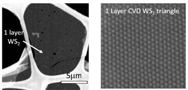
Transmission electron images (TEM) acquired from CVD grown WS2 (triangular) monolayers on c-cut sapphire confirming highly crystalline nature of monolayers
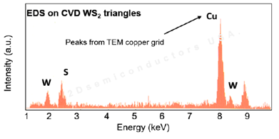
Energy dispersive X-ray spectroscopy (EDX) characterization on CVD grown full area coverage WS2 on sapphire confirming W:S 1:2 ratios
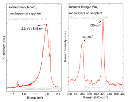
Room temperature photoluminescence spectroscopy (PL) and Raman spectroscopy (Raman) measurements performed on CVD grown full area coverage MoS2 monolayers on c-cut sapphire. Raman spectroscopy measurement confirm monolayer nature of the CVD grown samples and PL spectrum display sharp and bright PL peak located at 1.85 eV in agreement with the literature.


7天即到
本地发货
满500元
免运费

支持信用卡在线支付
和银行转账

客服电话:400-701-7100
Email: taizhou@sunano.com.cn
 陈谷一
陈谷一