

详情
This product contains tellurene monolayer, few-layer, and thicker flakes in isopropanol solution. Synthetic tellurene crystals has been first grown at 99.9995% purity, followed by dispersion into isopropanol (electronic grade chemical at 99.9999% purity) by ultrasonic treatment. Since the starting material (synthetic tellurene crystals) is highly crystalline, ultrasonic treatment to delaminate tellurene layers yields highly crystalline tellurene mono- and few-layers suspended in isopropanol solution. The crystallinity of tellurene nanomaterials has been confirmed by electron energy dispersive spectroscopy (EDAX), Raman spectroscopy (FWHM-1), and scanning electron microscopy (SEM) measurements. Lateral sizes of tellurene flakes deposited onto different substrates range from ~10nm - ~tens of microns.
Solution type: By default 2Dsemiconductors USA will provide tellurene sheets suspended in isopropanol owing to good dispersion, stability, and high performance. However, if your research requires other solvents, please contact us for more details and schedule for the product delivery.
Solution concentration: To reduce shipping costs, easy customs agreement / border check-in processes, we ship supersaturated 2D solutions (~80-120 mg/L depending on the type of 2D layers). However, supersaturated solutions can be diluted to produce ~250-500mL of solution to deposit 2D layers onto desired substrates through simple and cost-effective spin-casting process.
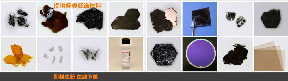
General characteristics of tellurene: Layered tellurium (Te) has a trigonal crystal lattice (see product images) in which individual helical chains of Te atoms are stacked together by van der Waals type bonds and spiral around axes parallel to the [0001] direction at the center and corners of the hexagonal elementary cell [1-2]. Tellurene exhibits a tunable bandgap varying from nearly direct 0.31 eV (bulk) to indirect 1.17 eV (2L) and direct at 1.3 eV (1L) [3]. It has been shown to exhibit metallic behavior under certain conditions and even host DCWs. It has four (two) complex, highly anisotropic and layer-dependent hole (electron) pockets in the first Brillouin zone with an extraordinarily high hole mobility reaching up to theoretical ∼1E5 cm2/Vs value [1-3].
High carrier mobility semiconductor
Tunable IR semiconductor (Eg ranging from 0.3 to 1.3 eV from bulk to monolayers)
2D anisotropic semiconductor
Note: This product is same as tellurene material. While material itself is perfectly crystallized in trigonal form (weakly coupled Te chains are present), it is inherently harder to exfoliate in comparison to graphene or MoS2. For best results, we recommend using strongly adhesive tapes or liquid exfoliation technique.
Frequently asked questions
Q1: Are these solutions good for catalytic measurements?
A: Yes, our 2D solutions are commonly used by catalysis community
Q2: What is the volume of the solution?
A: Each order can either contain 2mL of supersaturated monolayer solution (~200mg/L) or dense 20mL solutions (~20mg/L). We recommend using 2mL solutions as this will cut down the shipping charges and shipping times.
Q3: Are these 2D solutions consist of 100% monolayers?
A: This will depend on your requirements. We can design monolayer, few-layer, multi-layer, and even bulk layered solutions. Please identify what kind of solution (material type) you prefer to use during check out.
Q4: How about the solution types?
A: This will also depend on your application. We have capability to accommodate IPA, H2O, DMF, NMP, and many others. Just let us know what you have in mind.
Related references
[1] "Two-dimensional tellurium" Nature 552, 40-41 (2017) [Page link]
[2] "Large-area solution-grown 2D tellurene for air-stable, high-performance field-effect transistors"; arXiv:1704.06202 [Page link]
[3] "Few-layer Tellurium: one-dimensional-like layered elementary semiconductor with striking physical properties" ; https://doi.org/10.1016/j.scib.2018.01.010


7天即到
本地发货
满500元
免运费

支持信用卡在线支付
和银行转账

客服电话:400-701-7100
Email: taizhou@sunano.com.cn
 陈谷一
陈谷一